
Someone Split Your Computer In Half: And Somehow It Still Works
Why was your computer split in half? The gap that was never supposed to be.

Why are the CPU and RAM two different chips?
Genuinely. Who decided that? At some point someone drew a line down the middle of a computer, compute goes here and memory goes there and everyone just went with it. For almost Seventy years!
Turns out that one decision is why your computer works the way it does. And also why it doesn’t work as well as it should.
Last post we talked about the fallout. 200 clock cycles of your CPU doing absolutely nothing, just waiting for data to show up. Caches, prefetchers, multicore, Forty years of increasingly desperate workarounds for one mismatch that nobody fixed at the source.
And I ended with: the industry isn’t patching the gap anymore. It’s questioning whether the gap needs to exist at all. Took them long enough, but we’re getting there!
The Split?
Alright then, let’s start from the start! The question is genuine, why was the system even designed with a split? Why was the Processor and Memory split into two different chips and not kept as a single die of chip? Surely that’s the best way to do it isn’t it?
So who introduced the gap?
To answer this, we have to take a look back in the ages when the computers were still in the very fundamental development stages. Back in the mid-1940s, computers did not have the concept of stored program memory. Now you might ask how computers even functioned without memory and without the fundamental block of electronics, THE TRANSISTOR!
Well, it was different back then. Computers were purely computational machines, not the general-purpose ones they’ve become today. Back in the day, to perform the calculations, the computer needed to be programmed and reprogrammed for each such calculation. The ENIAC, an initial stage computer, had 20 accumulators storing 10-digit decimal numbers, but it had no program memory.
This meant unplugging the system, turning switches on and off according to the compute logic requirements, plugging back the system, just to find out that you mis-pressed the switches and do this all over again!
The Von Neumann
Pretty hectic for a few calculations, right? Yeah, the glass tubes were still used for compute so this was the only way. Later as the technology grew, so did the memory and the ways to store the instructions and the data.
Initially it was the Punch-Cards which were used to program the Computer externally without requiring it to be stopped, which could be stacked to grow the length of the instructions
This later grew into instructions now being stored magnetically on the Magnetic Drum. More importantly, they could be rewritten without creating an entirely new set of cards which aided with flexibility of programming.
Though, the final breakthrough came with the Electronic Random Access Memory. The data could be accessed without any moving parts, and thus could be accessed without any practical wait. More importantly, the data could be accessed randomly instead of sequentially like the previous inventions. That’s why it’s the Random Access Memory!
This led to what we today know as the Von Neumann Architecture, where both programs and instructions reside in the same memory and can be shared over the same path as required. This solved the problem of programmability since instructions just became data!
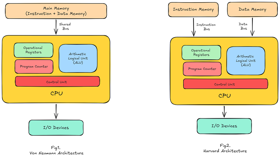
Fig1. Traditional Computer Architecture Layour
It was elegant and flexible, becoming the foundation for almost every general-purpose computer that followed. But because instructions and data shared the same memory and communication path, they also had to compete for it. To avoid this, the Harvard Architecture took a different approach by keeping instructions and data in separate memories with separate pathways, allowing both to be accessed independently.
The Actual Split
So both the architectures introduced the logical gap between the memory, but it was just supposed to be on the paper. Right? Then why’d the processor and the memory grew apart? Who split the damn Computer!?
Well, let’s not start blaming John Von Neumann and Computer Architects of that era, for it wasn’t their fault. They had been recently introduced to a new toy, the Transistor! By 1960s, with the invention of ICs, the form factor of the computer reduced significantly. From being comparable to a modern house, the ENIAC, to a handful of cabinets, the IBM 1401. This, alongside the reduction in power consumption from 150kW to around 10–15kW made it commercially feasible. This change was significant. Though very few overall, by the 1960s more than half of the computers worldwide were the IBM 1401s!
Meanwhile, requirements grew and so did the technology that fulfilled them. The processors required fast computing and the memory required more storage for the growing computing needs.
For the processor, it benefitted from high switching speeds and high performance transistors. Spending more silicon on higher compute speed was the right choice for the time being. Meanwhile, memory grew the other way. Spending more on the silicon area for compute meant lower area for the memory. Then how did the memory density increase?
With the invention of DRAM in early the 70s, memory density grew with the simple patented 1T1C (1 transistor 1 capacitor) cell, memory density skyrocketed. The single cell was tiny, scalable and ridiculously cheap to replicate billions of times, but it was never built with speed in mind.
Now putting these two technologies together on the same die meant compromising the compute speed for memory density or vice-versa, which would have limited the system’s performance significantly. The Physical Split became more and more prominent as the semiconductor technology evolved and the manufacturing processes for Processors and DRAM grew and drifted apart, significantly.
It was never a design choice someone made! It’s just how the technology grew around the system requirements!
The Consequence
So the system must have failed, right? Well, it worked brilliantly! For now. Memory capacities grew, processors became more powerful, and nobody had any reason to question anything.
And obviously, then came the Moore’s Law. Everything was working and growing, but maybe not proportionately. The Memory Gap started forming. Surely someone noticed and did something about it, right?
Well, each generation kept growing faster. The hardware benchmarks were improving, the software quality was rising and the system was growing overall. The gap hid under the overall growth, and because everything was growing there was nothing to complain about
As time moved on, so did the gap. But the engineers weren’t blind to it. They responded with Caches, Prefetchers, Out-Of-Order Execution, Branch Prediction and Deeper Memory Hierarchies, all designed to keep the processor busy while it waited for data. Instead of solving the problem, they became increasingly sophisticated ways of hiding it.
For decades, these techniques worked well enough. But they all shared one assumption: the data would still live somewhere else, and the processor would eventually have to go fetch it, which was affected by the choices made previously. As processors continued to outpace memory, the cost of moving data slowly began to rival, and often exceed, the cost of computing on it.
This was made visible in 1995 when Wulf and McKee formally described what they called The Memory Wall. Their analysis showed that processor performance was improving far faster than memory latency could keep up, meaning an increasing fraction of execution time was being spent simply waiting for data to arrive.
For the first time, the problem had a name. And once it had a name, the obvious question followed: if moving data was becoming more expensive than processing it, why keep moving it at all?
The Attempt and Failure
After the paper hit the industry by laying out the reality, the obvious question caught attention of the Computer Architects in the research labs. Why not move computation to the data instead?
The funny part is, this wasn’t even a new idea. As early as the 1970s, researchers had experimented with architectures that placed simple processing elements alongside memory to exploit massive parallelism. The 1990s saw another wave of proposals, from projects like TERASYS to Computational RAM, all built around the same philosophy: if moving data was expensive, stop moving it.
Yet none of them found widespread adoption. The hardware of the time simply wasn’t on their side. DRAM processes were optimized to pack as many bits as possible, not to accommodate logic, making integrated designs expensive and inefficient. At the same time, Caches kept getting larger, Processors kept getting faster, and clever architectural tricks were good enough to hide the growing problem for a while longer. There was little incentive to embrace a radical redesign when the existing approach still seemed to work.
So the idea quietly faded into the background. Not because it was wrong, but because it had arrived decades before the technology and the economics were ready for it.
The Perfect Timing
The real breakthrough wasn’t a new algorithm or a revolutionary architecture. It was the memory itself.
For decades, DRAM remained the workhorse of computing, optimized to store as many bits as possible at the lowest possible cost. That level of optimization was making it harder to shrink it’s size, leaving very small room for integrating logic, making the early Process-In-Memory proposals expensive and not feasible.
By the start of the new millennium, a shift was underway in memory technology. The development of 3D-Stacked Memory such as High Bandwidth Memory (HBM) and Hybrid Memory Cube (HBC). This technology allowed multiple DRAM layers to be stacked vertically, effectively increasing memory density and shrinking the distance between the Processor and the Memory. This was made possible using the Through-Silicon Vias (TSVs), enabling enormous internal bandwidth.
Alongside DRAM, fundamentally new ways of storing data were being developed too. The Spin-Transfer-Torque-Magnetic-RAM (STT-MRAM) is a non-volatile memory that replaced electric charge with magnetic states to store information. It wasn’t designed with compute in mind, but instead it challenged the fundamental idea behind DRAM, using electric charge to store data which required refreshing the tiny capacitors thousands of times every second. If this ever becomes cheaper and scalable, it should essentially be able to replace the DRAM, completely redefining what the Memory looks like!
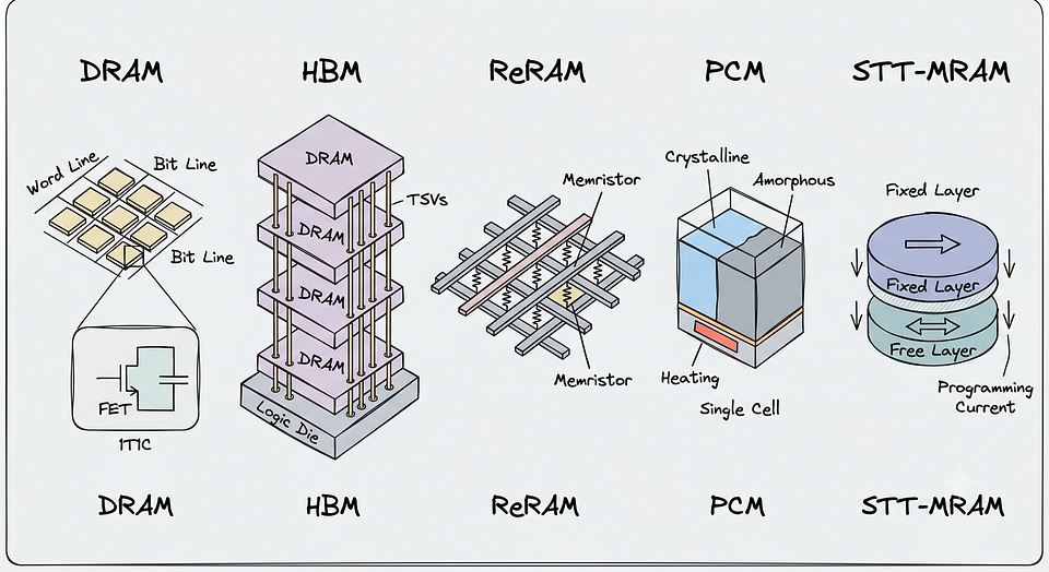
Fig2. Modern Memory Types
Some other approaches, like Resistive-RAM (ReRAM) and Phase Change Memory (PCM), just blurred the lines between storage and compute. Instead of representing data asmere binary values, their cells exploit the analog electrical properties of the materials! These characteristics can be directly used to perform mathematical operations! This Analog Computation is a growing area of study, which is made possible due to these memory technologies which use analog properties of materials, like Resistance in ReRAM and changing the entire material states between Crystalline and Amorphous like they do in PCM!
This has marked the beginning of this radical idea that perhaps the future is not about processors closer to the memory but trying to make them one. This, in fact, challenges one of the most fundamental assumptions that computation has to be digital, giving rise to Analog Computation! But that’s a story to explore for another day…
For now, the hardware was no longer standing between the idea of unifying the Processor and the Memory into a single unit!
For the first time, the question is no longer “Can we do it?
It has quietly become, “How do we do it?”
And turns out, the solution isn’t just a one-off trick, it’s an entire family of ideas, each trying to bring the Processor and the Memory closer!
The Inversion
Now that we have established that moving the Compute nearer to the Memory is no longer just an idea but a possible reality, different people interpret the idea differently, producing a whole family of solutions for the same problems. This family of solutions is each built around a different interpretation.
Process Near Memory (PNM)
The most obvious interpretation one might think of. Instead of changing the Memory itself, literally move the Processor closer to it. Dedicated logic, CPU Cores and Accelerators placed alongside the Memory Chips, often on the HMB or HMC.
This feels like a small change and not really a radical justification to the idea, but this small change allows the Processor to access the Internal Bandwidth of a HBM or HBC of up to 500GB/s, compared to the 50GB/s of the typical off-chip connection.
The Von Neumann Architecture still stands, the Memory and the Processor are physically apart but what makes this brilliant is that it doesn’t demand a fundamental change in the way we store data but works with what already exists and exploits that to it’s greatest strengths!
Process In Memory (PIM)
PIM brings the idea closer to it’s interpretation according to it’s name. Why even keep them apart if they are just so close to each other?
The Compute logic directly embedded inside the Memory, small ALUs, MAC Engines (Multiply and Accumulate) which is one of the most common operations in computing, Vector Units directly in the Memory Banks or Row-Buffer regions which is responsible for performing the same operation on many pieces of data simultaneously!
Samsung’s HBM-PIM is the commercial version of this. Lightweight Compute Engines directly compute where the data already is. The Von Neumann Architecture is breaking now, the Processor and the Memory are becoming one single Compute-Memory-Workhorse!
Process Using Memory (PUM)
This is where the idea completely blows out of proportion. PNM moved the Processor closer to the Memory. PIM embedded the logic inside the Memory.
PUM asks a question that almost sounds too offensive the first time you hear it:
“What if you don’t need the processor at all?”
What if the physical behavior of the Memory Cells perform the computation on their own, no dedicated logic required. No Fetch. No Writeback. No processor Involvement. Turns out it’s happening already.
Take Ambit, a research prototype that exploits how DRAM cells electrically interact when multiple rows are activated simultaneously. Activate the rows in the right sequence and it returns the result of a Logical Operation on the data. The AND, OR, NOT logic, without a single instruction once reaching the processor. And if you know even a little bit Computers, you might know that it’s all that takes to do any calculation!
ReRAM goes even further, it’s crossbar arrays perform the Matrix-Vector-Multiplications as a natural result of how the electrical resistance distributes across the grid. You don’t program it to compute, it computes because of it’s physical consequence!
The But
Now that the Processor and the Memory can be merged into one single unified block of data and computation, you might think that’s it! Problem solved! We combine the Processor and the Memory, no Latency Issues, no Memory Gap and thus peak computation achieved!
Well, hate to break it to you, it won’t work out like that. PIM was designed to fix one very specific problem, The Memory Gap, where the bottleneck isn’t how fast you can compute, but how fast you can feed data to the compute unit in the first place.
The technical term for this is Low Arithmetic Intensity. For every byte being moved, very little Math needs to be done. That’s exactly where PIM hits hardest, large movement of data for a relatively low level of compute.
But here’s where it gets honest. PIM is genuinely good at what it was designed for, bitwise operations, integer arithmetic, bulk data movement. Ask it to do floating point and you’re often looking at emulation that quietly eats the gains you came for. Most implementations also can’t talk to each other efficiently, no low-latency interconnects between compute units, which becomes a problem the moment your workload needs any coordination across the array.
The software story is worse. No unified programming model. Compiler support that’s still finding it’s feet. Vendor-specific APIs that don’t talk to each other. And cache coherence, when PIM modifies memory directly while the CPU cache holds a stale copy of the same address, remains an open problem that current research only partially solves.
Turns out, questioning a Seventy-year-old assumption is easier than adopting the whole system around it!
Conclusion
So as we come to an end of this discussion, why are the CPU and RAM two different chips? Why did the idea of not keeping the Processor and the Memory apart come back alive? Because of The Memory Gap, duh!
We discussed the history of why these two were apart in the first place. And somehow why computers still worked without memory, primitively, and then even with the gap between them! Well, it worked, and that’s what caused the issues. How the industry kept applying patches around it instead of attacking the root cause, bringing the Processor and the Memory closer, or even as a single unified component for once!
How the tech lagged behind the idea. And once the tech caught up, how the idea moved in a completely different direction than what it was initially supposed to? How the industry spent seven decades questioning the premise and another four decades along the way to develop and implement the technology, and still isn’t complete!
PIM might become the foundation of the next era of computing. It might turn out to be the brilliant idea that just arrived too early, or even that one that seemed too promising at first but didn’t work out as expected. Nobody knows yet.
One thing’s for sure, the development it brought alongside it’s research in memory and memory types has laid a path for Analog Computing once again. Once again? Yes, turns out computing used to be analog initially. Surprising, right? Well, that’s something to explore for the next turn.
Until then, keep exploring. It’s all just curiosity and a keyboard after all!
